energy band diagram of pn junction diode pdf
This ability to change conductivity with the amount of applied voltage can be used for. The metaloxidesemiconductor field-effect transistor MOSFET MOS-FET or MOS FET is a type of field-effect transistor FET most commonly fabricated by the controlled oxidation of siliconIt has an insulated gate the voltage of which determines the conductivity of the device.

Tunnel Diode Definition Symbol And Working Diode
The wave functions have been drawn so that their zeros are at the corresponding energy levels.

. Therefore the band gap is the. It is a PN- junction diode which emits light when activated. A diode vacuum tube or thermionic diode is a vacuum tube with two electrodes a heated cathode and a plate in which electrons can flow in only one direction.
The maximum electrical power P elmax that can be supplied to an LED is limited by the maximum pn-junction. The light produced from a light emitting diode LED is the most obvious example of radiative recombination in a semiconductor device. Reducing depletion width can be inferred from the shrinking carrier motion across the pn junction which as a consequence reduces electrical.
Energy in the Coulomb case. Energy Band Diagram of Schottky Contact. From the diagram we can see that the band around the package corresponds to the line on the diode circuit symbol and this can be an easy way of remembering which end is for which.
HUGHES ELECTRICAL AND ELECTRONIC TECHNOLOGY ELEVENTH EDITION. 346 wt NH 4F 68 wt HF 586 H20 TABLE 2 lists physical properties of SiO2 and Si3N4. A diode is a two-terminal electronic component that conducts current primarily in one direction asymmetric conductance.
Zener diodes are manufactured with a great variety of Zener voltages and some are even variable. It is a form of photoelectric cell defined as a device whose electrical characteristics such as current voltage or resistance vary when exposed to light. Etch rate in Buffered HFa Åmin 1000 5-10 a Buffered HF.
Those that rely solely on purely macroscopic properties and. Both p and n junctions are doped at a 1e15 cm -3 160 µCcm 3 doping level leading to built-in potential of 059 V. Each band diagram corresponds to a distinct carrier injection into the ETH device.
The explanation behind the emission of photons in an LED diode lies in the energy band theory of solids. Cohesive energy and bond strength increase rapidly and control of the electronic. The Zener diode has a reverse-breakdown voltage at which the diode starts conductivity electric current and remains continuous in the reverse-bias mode.
US2524035A US33466A US3346648A US2524035A US 2524035 A US2524035 A US 2524035A US 33466 A US33466 A US 33466A US 3346648 A US3346648 A US 3346648A US 2524035 A US2524035 A US 2524035A Authority US United States Prior art keywords electrode collector emitter block current Prior art date 1948-02-26 Legal status The legal status is an assumption. Solar-energy conversion and light emission in an atomic monolayer pn diode. Animation giving a graphical represenation of recombination mechanisms.
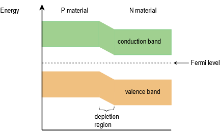
There are three types of temperature scale. Doping a semiconductor in a good crystal introduces allowed energy states within the band gap but very close to the energy band that corresponds to the dopant typeIn other words electron donor impurities create states near the conduction band while electron acceptor impurities create states near the valence band. The band gap E G is the gap in energy between the bound state and the free state between the valence band and conduction band.
Electronic Communication System 4th Edition by Kennedy Davispdf. Sensors are essential components of automotive electronic control systems. With a type II junction band alignment where the bottom of the conduction and the top of the valence bands reside in different layers an external electric field from the gate can modulate the.
ELECTRONICS COMMUNICATION SYSTEM BY GEORGE KENNEDYpdf. The photovoltaic effect is closely related to the photoelectric effectFor both phenomena light is absorbed causing excitation of an electron or other charge carrier to a higher-energy state. Those such as the SI scale that are defined in terms of the average translational kinetic energy per freely moving microscopic particle such as atom molecule or electron in a body.
A photodiode is a fast highly linear device that exhibits high quantum efficiency and may be used in a variety of different applications. Radiative recombination is the recombination mechanism that dominates in direct bandgap semiconductors. ELECTRONICS COMMUNICATION SYSTEM BY GEORGE KENNEDYpdf.
The gap between these energy states and the nearest energy. According to this theory whether the electron-hole combining will give out photons or not depends on whether the material has a direct band gap or indirect band gap. The main distinction is that the term.
Multi-junction MJ solar cells are solar cells with multiple pn junctions made of different semiconductor materialsEach materials p-n junction will produce electric current in response to different wavelengths of lightThe use of multiple semiconducting materials allows the absorbance of a broader range of wavelengths improving the cells sunlight to electrical. It has low ideally zero resistance in one direction and high ideally infinite resistance in the other. The photovoltaic effect is the generation of voltage and electric current in a material upon exposure to lightIt is a physical and chemical phenomenon.
HUGHES ELECTRICAL AND ELECTRONIC TECHNOLOGY ELEVENTH EDITION. A solar cell or photovoltaic cell is an electronic device that converts the energy of light directly into electricity by the photovoltaic effect which is a physical and chemical phenomenon. The lower energy level of a semiconductor is called the valence band E V and the energy level at which an electron can be considered free is called the conduction band E C.
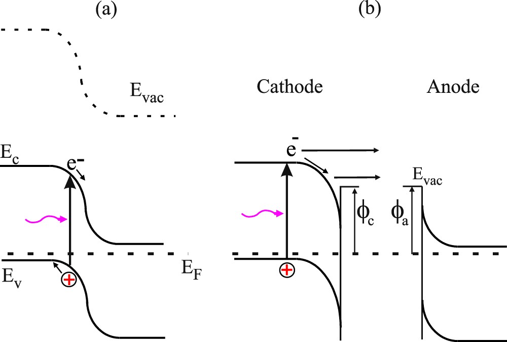
A junction photodiode is an intrinsic device that behaves similarly to an ordinary signal diode but it generates a photocurrent when light is absorbed in the depleted region of the junction semiconductor. Note that the zero of energy corresponds to the top line in the diagram. Physical Constants Symbol Name Value q magnitude of electronic charge 1602 x 10-19 C M0 electron mass in free space 9109 x 10-31 kg Eo permittivity of vacuum 8854 x 10-14 Fcm k Boltzmanns constant.
Temperature is a physical quantity that expresses the hotness of matter or radiation. Some Zener diodes have a sharp highly doped pn junction with a low Zener voltage in which case the. The diode usually consists of a p-n junction which is heavily doped.
I think it will be helpful for the public. Energy states in the bandgap at the metal-semiconductor interface pins Ef to a range of 04 eV to 09 eV below Ec. The diode is designed to conduct the flow of current in the reverse direction after reaching a specified voltage.
A Zener diode is a special type of diode designed to reliably allow current to flow backwards when a certain set reverse voltage known as the Zener voltage is reached. HUGHES ELECTRICAL AND ELECTRONIC TECHNOLOGY ELEVENTH EDITION. I0 of a Schottky diode is 103 to 108 times larger than a PN junction diode depending on.
The diagram shows the potential energy along with the four lowest energy levels and the wave functions corresponding to the lowest two of these. The panels show energy band diagram electric field and net charge density. Individual solar cell devices are often the.
The Zener diode circuit symbol places two tags at the end of the bar one in the upward direction and the other in the lower direction as shown in the figure. Sensors are defined as devices that transform or transduce physical quantities such as pressure or acceleration called measurands into output signals usually electrical that.
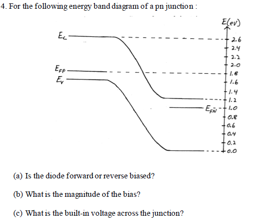
Solved 4 For The Following Energy Band Diagram Of A Pn Chegg Com

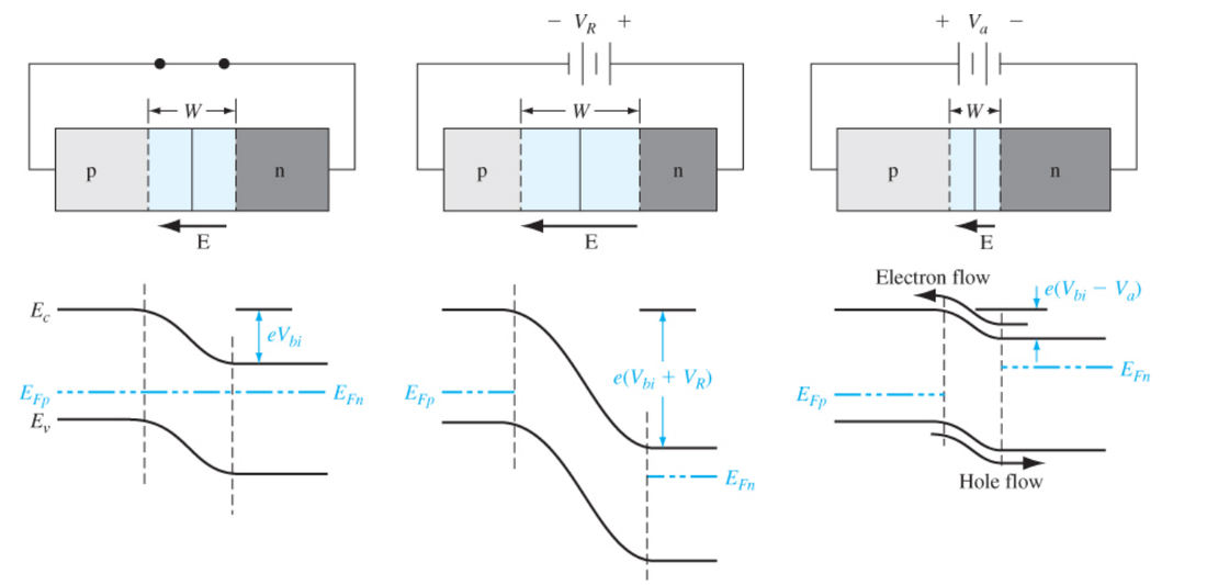
Biasing Of P N Junctions
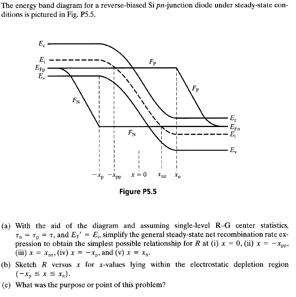
The Energy Band Diagram For A Reverse Biased Si Chegg Com

Tunnel Diode Working And Characteristics Electronics Club

Energy Band Diagram An Overview Sciencedirect Topics
Understanding The Second Approximation Of Diodes Physics Forums

P N Junction Energy Band Gap
Pn Junction Diode Springerlink

Pn Junctions Worksheet Discrete Semiconductor Devices And Circuits
Electronic Devices 2016 Inderjit Singh

Homojunction An Overview Sciencedirect Topics

Energy Band Diagram An Overview Sciencedirect Topics
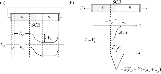
2 2 The Pn Junction Engineering Libretexts
Problem 4 25 Marks The Energy Band Diagram For A Reverse Biased Course Hero
Solar Energy Converters Based On Multi Junction Photoemission Solar Cells Scientific Reports
A Sketch Of The Energy Band Structure Of A P N Junction Containing A Download Scientific Diagram

Energy Band Diagram In Forward Bias And Reverse Bias For A P N Junction Download Scientific Diagram